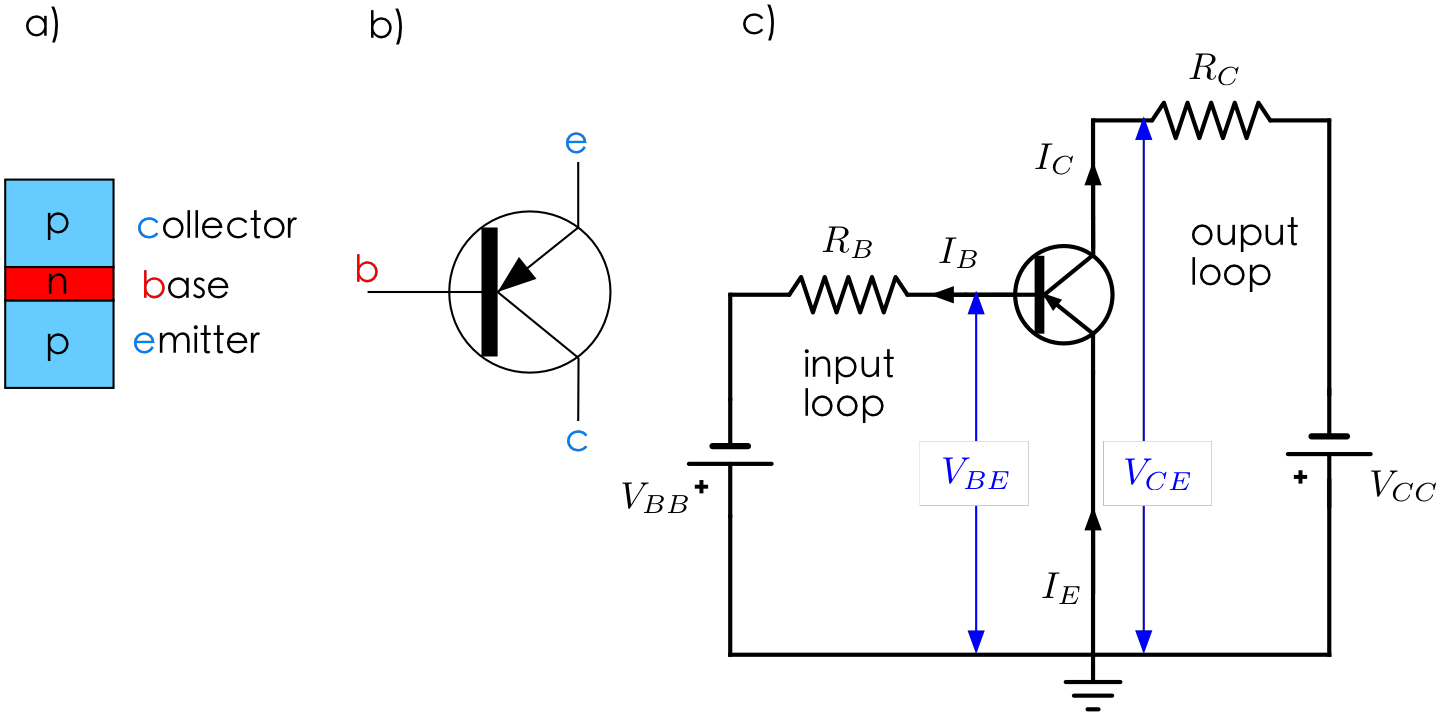
Biasing Of Transistor Collector . Our transistor biasing calculator will help you discover and understand. Operation can only be obtained when the transistor spends its entire time in the active mode, never reaching either cutoff or saturation. To achieve this, sufficient dc. The collector characteristic curves for this transistor are shown in fig. Web transistor biasing is the process of setting a transistor’s dc operating voltage or current conditions to the correct. 2 (a) is biased with v cc and v bb to obtain certain values of i b, i c, i e, and v ce. Web transistor biasing is defined as the proper flow of zero signal collector current and the maintenance of proper collector emitter voltage. Web the transistor in fig. Web transistor biasing (cont) we're continuing on in chapter 10 with the subject of. Web transistors (and their offsprings) are a fundamental part of every electronic device: Although transistor switching circuits operate without bias, it is unusual for analog circuits.
from wanda.fiu.edu
Web the transistor in fig. 2 (a) is biased with v cc and v bb to obtain certain values of i b, i c, i e, and v ce. Our transistor biasing calculator will help you discover and understand. The collector characteristic curves for this transistor are shown in fig. Web transistor biasing is defined as the proper flow of zero signal collector current and the maintenance of proper collector emitter voltage. Web transistors (and their offsprings) are a fundamental part of every electronic device: Although transistor switching circuits operate without bias, it is unusual for analog circuits. To achieve this, sufficient dc. Operation can only be obtained when the transistor spends its entire time in the active mode, never reaching either cutoff or saturation. Web transistor biasing is the process of setting a transistor’s dc operating voltage or current conditions to the correct.
26. Transistor Characteristics — Modern Lab Experiments documentation
Biasing Of Transistor Collector Web transistor biasing is defined as the proper flow of zero signal collector current and the maintenance of proper collector emitter voltage. Operation can only be obtained when the transistor spends its entire time in the active mode, never reaching either cutoff or saturation. Web the transistor in fig. Web transistor biasing is defined as the proper flow of zero signal collector current and the maintenance of proper collector emitter voltage. Web transistor biasing is the process of setting a transistor’s dc operating voltage or current conditions to the correct. 2 (a) is biased with v cc and v bb to obtain certain values of i b, i c, i e, and v ce. Although transistor switching circuits operate without bias, it is unusual for analog circuits. To achieve this, sufficient dc. Our transistor biasing calculator will help you discover and understand. Web transistors (and their offsprings) are a fundamental part of every electronic device: Web transistor biasing (cont) we're continuing on in chapter 10 with the subject of. The collector characteristic curves for this transistor are shown in fig.
From www.cahani.com
Are comparisons may don were if required them, chart this medium DOA Biasing Of Transistor Collector Web the transistor in fig. Our transistor biasing calculator will help you discover and understand. The collector characteristic curves for this transistor are shown in fig. Web transistors (and their offsprings) are a fundamental part of every electronic device: Web transistor biasing is the process of setting a transistor’s dc operating voltage or current conditions to the correct. Web transistor. Biasing Of Transistor Collector.
From hackaday.com
Biasing That Transistor The Common Emitter Amplifier Hackaday Biasing Of Transistor Collector 2 (a) is biased with v cc and v bb to obtain certain values of i b, i c, i e, and v ce. Although transistor switching circuits operate without bias, it is unusual for analog circuits. Web transistors (and their offsprings) are a fundamental part of every electronic device: Web the transistor in fig. Web transistor biasing is defined. Biasing Of Transistor Collector.
From www.circuitbread.com
Bipolar Junction Transistor (BJT) Basics CircuitBread Biasing Of Transistor Collector Operation can only be obtained when the transistor spends its entire time in the active mode, never reaching either cutoff or saturation. Web the transistor in fig. Our transistor biasing calculator will help you discover and understand. The collector characteristic curves for this transistor are shown in fig. Web transistor biasing (cont) we're continuing on in chapter 10 with the. Biasing Of Transistor Collector.
From www.theengineeringknowledge.com
Transistor Biasing Method The Engineering Knowledge Biasing Of Transistor Collector Web transistor biasing is the process of setting a transistor’s dc operating voltage or current conditions to the correct. Web transistors (and their offsprings) are a fundamental part of every electronic device: Web transistor biasing (cont) we're continuing on in chapter 10 with the subject of. The collector characteristic curves for this transistor are shown in fig. 2 (a) is. Biasing Of Transistor Collector.
From www.circuitbread.com
Transistor Bias Circuits Study Guides CircuitBread Biasing Of Transistor Collector Web the transistor in fig. Web transistor biasing (cont) we're continuing on in chapter 10 with the subject of. Although transistor switching circuits operate without bias, it is unusual for analog circuits. Our transistor biasing calculator will help you discover and understand. Web transistors (and their offsprings) are a fundamental part of every electronic device: To achieve this, sufficient dc.. Biasing Of Transistor Collector.
From www.slideserve.com
PPT PNP transistor (structure, operation, models) PowerPoint Biasing Of Transistor Collector 2 (a) is biased with v cc and v bb to obtain certain values of i b, i c, i e, and v ce. To achieve this, sufficient dc. Web transistor biasing is defined as the proper flow of zero signal collector current and the maintenance of proper collector emitter voltage. Our transistor biasing calculator will help you discover and. Biasing Of Transistor Collector.
From www.researchgate.net
1 Common emitter self biased transistor amplifier circuit Download Biasing Of Transistor Collector Our transistor biasing calculator will help you discover and understand. 2 (a) is biased with v cc and v bb to obtain certain values of i b, i c, i e, and v ce. The collector characteristic curves for this transistor are shown in fig. Web transistor biasing is defined as the proper flow of zero signal collector current and. Biasing Of Transistor Collector.
From www.nutsvolts.com
Nuts & Volts Magazine For The Electronics Hobbyist Biasing Of Transistor Collector Web the transistor in fig. 2 (a) is biased with v cc and v bb to obtain certain values of i b, i c, i e, and v ce. Web transistors (and their offsprings) are a fundamental part of every electronic device: Although transistor switching circuits operate without bias, it is unusual for analog circuits. Operation can only be obtained. Biasing Of Transistor Collector.
From www.allaboutcircuits.com
Bipolar Junction Transistors Solidstate Device Theory Electronics Biasing Of Transistor Collector Operation can only be obtained when the transistor spends its entire time in the active mode, never reaching either cutoff or saturation. Although transistor switching circuits operate without bias, it is unusual for analog circuits. 2 (a) is biased with v cc and v bb to obtain certain values of i b, i c, i e, and v ce. Web. Biasing Of Transistor Collector.
From electronics.stackexchange.com
transistors How is the CollectorBase region reverse biased in Common Biasing Of Transistor Collector The collector characteristic curves for this transistor are shown in fig. Operation can only be obtained when the transistor spends its entire time in the active mode, never reaching either cutoff or saturation. Our transistor biasing calculator will help you discover and understand. Web transistors (and their offsprings) are a fundamental part of every electronic device: Although transistor switching circuits. Biasing Of Transistor Collector.
From www.allaboutcircuits.com
Transistor Biasing Calculations Bipolar Junction Transistors Biasing Of Transistor Collector Although transistor switching circuits operate without bias, it is unusual for analog circuits. Web transistor biasing is the process of setting a transistor’s dc operating voltage or current conditions to the correct. Web the transistor in fig. Our transistor biasing calculator will help you discover and understand. Operation can only be obtained when the transistor spends its entire time in. Biasing Of Transistor Collector.
From electronics.stackexchange.com
transistors The advantage of using base biasing over emitter biasing Biasing Of Transistor Collector To achieve this, sufficient dc. Our transistor biasing calculator will help you discover and understand. Web the transistor in fig. Operation can only be obtained when the transistor spends its entire time in the active mode, never reaching either cutoff or saturation. 2 (a) is biased with v cc and v bb to obtain certain values of i b, i. Biasing Of Transistor Collector.
From www.slidemake.com
Transistor Biasing And Stabilization Techniques Presentation Biasing Of Transistor Collector Our transistor biasing calculator will help you discover and understand. The collector characteristic curves for this transistor are shown in fig. Operation can only be obtained when the transistor spends its entire time in the active mode, never reaching either cutoff or saturation. Web transistor biasing is defined as the proper flow of zero signal collector current and the maintenance. Biasing Of Transistor Collector.
From exowbryvk.blob.core.windows.net
Biasing Of A Transistor Methods at Katherine Hayes blog Biasing Of Transistor Collector Web transistor biasing is the process of setting a transistor’s dc operating voltage or current conditions to the correct. Our transistor biasing calculator will help you discover and understand. The collector characteristic curves for this transistor are shown in fig. Web the transistor in fig. To achieve this, sufficient dc. Web transistor biasing (cont) we're continuing on in chapter 10. Biasing Of Transistor Collector.
From www.youtube.com
Collector Feedback Bias Circuit YouTube Biasing Of Transistor Collector Web the transistor in fig. Web transistor biasing is the process of setting a transistor’s dc operating voltage or current conditions to the correct. Web transistors (and their offsprings) are a fundamental part of every electronic device: To achieve this, sufficient dc. Web transistor biasing (cont) we're continuing on in chapter 10 with the subject of. Our transistor biasing calculator. Biasing Of Transistor Collector.
From exoqfbzus.blob.core.windows.net
Transistor Voltage Divider Biasing at John Lyons blog Biasing Of Transistor Collector Web transistor biasing (cont) we're continuing on in chapter 10 with the subject of. Web transistors (and their offsprings) are a fundamental part of every electronic device: Web transistor biasing is the process of setting a transistor’s dc operating voltage or current conditions to the correct. Web the transistor in fig. To achieve this, sufficient dc. 2 (a) is biased. Biasing Of Transistor Collector.
From electricalworkbook.com
What is Transistor Biasing? Circuit Diagram & Types (Fixed Bias Biasing Of Transistor Collector Operation can only be obtained when the transistor spends its entire time in the active mode, never reaching either cutoff or saturation. Web transistor biasing (cont) we're continuing on in chapter 10 with the subject of. 2 (a) is biased with v cc and v bb to obtain certain values of i b, i c, i e, and v ce.. Biasing Of Transistor Collector.
From ecstudiosystems.com
Vol. III Semiconductors Bipolar Junction Transistors Biasing Biasing Of Transistor Collector The collector characteristic curves for this transistor are shown in fig. Operation can only be obtained when the transistor spends its entire time in the active mode, never reaching either cutoff or saturation. Web transistor biasing is defined as the proper flow of zero signal collector current and the maintenance of proper collector emitter voltage. Web transistor biasing (cont) we're. Biasing Of Transistor Collector.